
Samsung Made $75 Billion in One Quarter. The Reason Is 12 Chips Stacked Into One.
One Bad Chip Scraps the Whole Stack: The Maths Behind the AI Memory Boom
In plain words
On 8 October 2026 Samsung said it made about $75 billion in one quarter. The reason: 12 chips stacked into one.
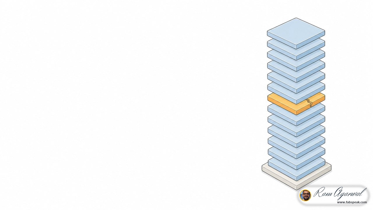
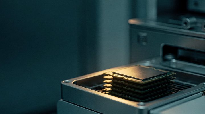
The memory beside every AI chip is a tower: a base chip with 12 memory chips stacked on top.
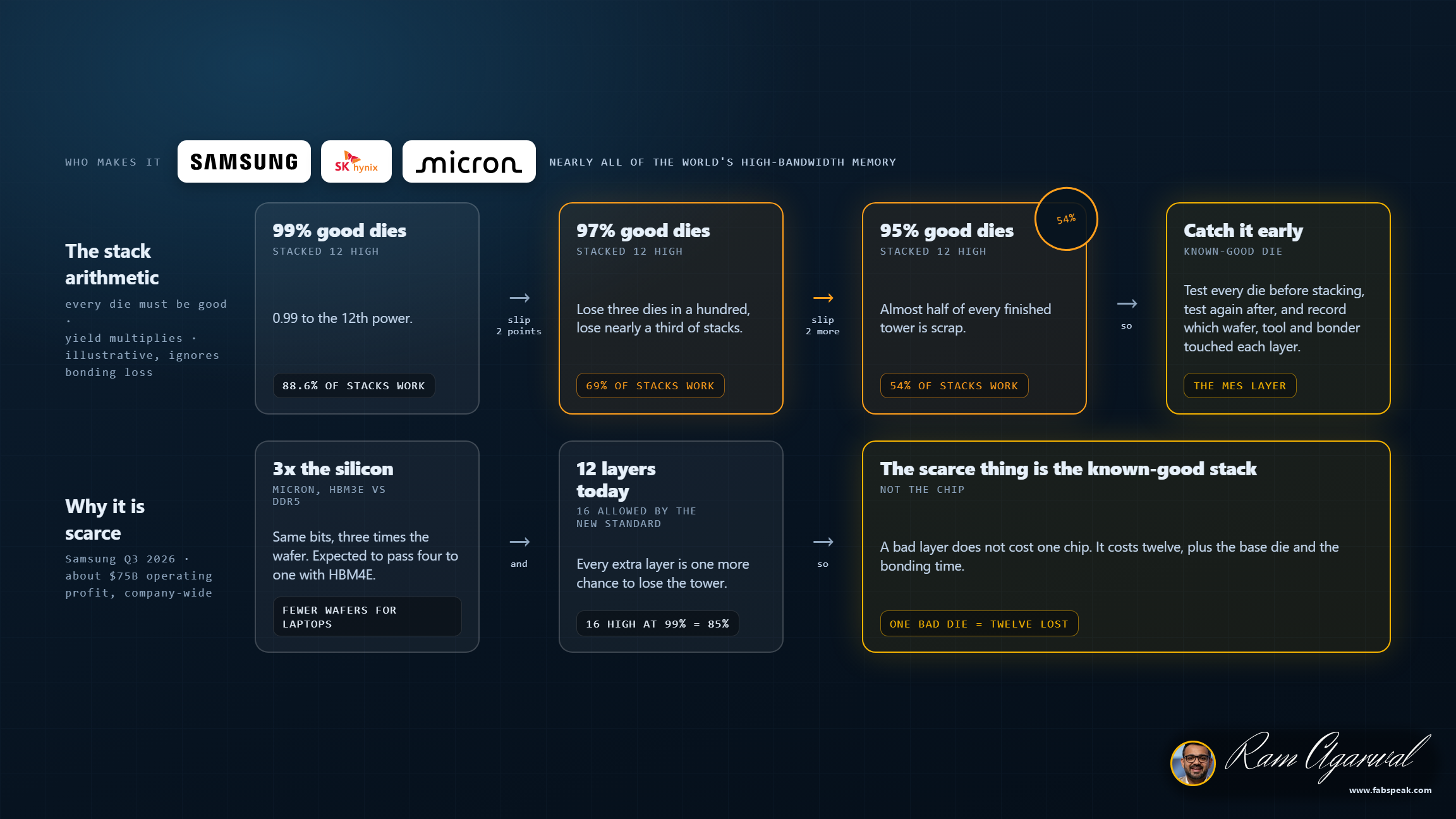
Micron says that tower needs about three times the silicon of normal memory to hold the same data.
One bad layer means the whole tower is thrown away, so at 99% good per chip only about 88.6% of 12-high towers work.
Samsung, SK hynix and Micron test every chip before it goes in, test again after, and trace it back to its wafer and machine.
A rule book for that tracking, called SEMI E142, has existed since 2006. The next towers will be 16 high, so it matters more.
Picture it. It is like a twelve-storey building where one bad floor means demolishing the whole thing. You inspect every floor before it goes up, because finding a problem on the roof costs eleven floors.
Why it matters to you. The scarce thing in AI memory is not the chip. It is the tower where every layer is good. Ask where in your own process a defect is cheapest to catch.
Terms in this piece
- SEMI SEMI, the semiconductor equipment and materials industry association
- The industry body whose standards say how fab equipment talks, reports and is measured.
The number
OF 12-HIGH STACKS WORK AT 99% PER DIE, 2026
What to do Monday
Pick one step in your process, and ask what it costs to catch a defect there, versus two steps later. That ratio is your whole yield strategy. Why it works: in any multi-step process, the cost of a defect grows with every step it survives, because each later step adds value to something that is already scrap. In a twelve-high memory stack the multiplier is brutal, but the same logic holds on any line. Write down one step, the cost of catching a defect there, and the cost two steps later. The gap tells you where inspection pays.
The honest caveat
The stack percentages are arithmetic, not any company's reported yield: they assume each chip fails independently and ignore losses in the joining step, which make real numbers worse. Samsung's figure is company-wide operating profit and covers a different period from NVIDIA's, so the comparison is for scale only.
Your turn
Where in your process would catching a defect one step earlier save the most?
Argue with me on LinkedInSources
- PrimarySamsung Electronics, "Earnings Guidance for Third Quarter 2026", 8 October 2026 [primary]: consolidated operating profit of approximately KRW 107.4 trillion on sales of approximately KRW 195 trillion - https://www.samsung.com/global/ir/reports-disclosures/public-disclosure-view.84775/ link
- PrimaryNVIDIA, Q2 fiscal 2027 results, quarter ended 26 July 2026 [primary]: revenue of $96.2 billion and operating income of $63.7 billion - https://www.sec.gov/Archives/edgar/data/0001045810/000104581026000073/q2fy27pr.htm link
- PressMicron, fiscal Q2 2025 commentary (Blocks and Files, March 2025) [primary via press]: HBM3E consumes about three times the silicon of DDR5 for the same bits; the trade ratio rises with HBM4 and is expected to exceed four to one with HBM4E - https://blocksandfiles.com/2025/03/21/micron-q2-fy25-2/ link
- PrimaryUtmel, "2026 DRAM and the 3-to-1 HBM rule" (2026) [industry reference]: the wafer trade ratio's effect on conventional DRAM supply - https://www.utmel.com/blog/categories/memory%20chip/2026-dram-and-the-3-to-1-hbm-rule-market-supply-analysis-and-b2b-procurement-guide link
- PrimaryStack-yield arithmetic [worked example, not company data]: 0.99^12 = 0.886; 0.97^12 = 0.694; 0.95^12 = 0.540; 0.99^16 = 0.851. Assumes independent die failures and no bonding loss.
- PrimarySEMI E142, "Specification for Substrate Mapping" (first published 2006) [standard]: the data model for tracking individual devices through assembly - https://store-us.semi.org/products/e14200-semi-e142-specification-for-substrate-mapping link
Read the full script (235 words)
Keep reading
All pieces
SK hynix, Intel's Ohio Fab, and the Rule That Copies the Plumbing
On 16 September 2026 Reuters reported that SK hynix, the world's biggest maker of the memory inside AI chips, is in talks with Intel about making memory chips in the United States for the first time: either by leasing part of Intel's $28 billion campus in Ohio, or through a joint venture with Intel and…
The Chip So Big They Can't Throw the Broken Part Away
Every chip factory on Earth runs on the same rule: cut the wafer into hundreds of chips, test them, and throw the broken ones away. That rule is what "yield" means.
AI Ate Your RAM — And There Was Never a Shortage
Your RAM got about twice as expensive this year, and the reason has almost nothing to do with a shortage — the memory fabs are running flat out at record output, with $52B going into 300mm memory equipment in 2026 alone, up 29%. What actually happened is a reallocation, and it comes down to physics…