
Two AI Labs Shipped Models This Week. A Chip Factory Was Reading 12 Characters.
Every Chip Has a Name Before It Exists. The Factory Spends 3 Months Trying Not to Lose It.
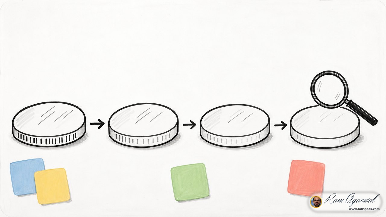
In plain words
Two AI labs each shipped a new model on Tuesday. A chip factory spent the week reading twelve characters.
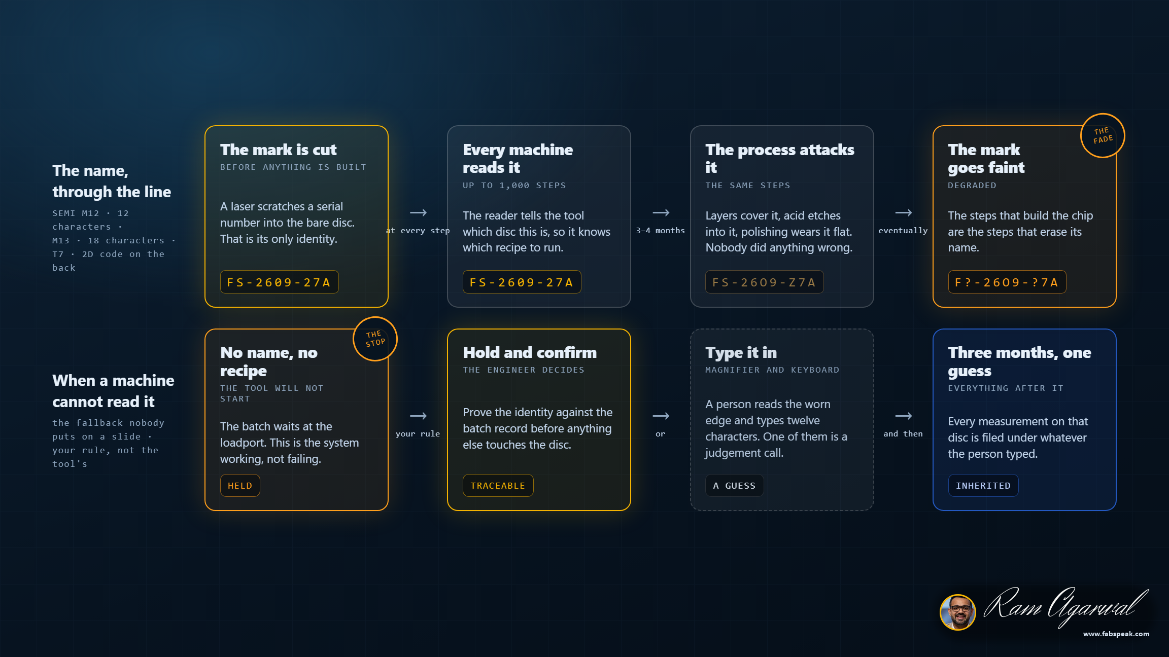
A wafer is a mirror-smooth disc of silicon. Before anything is built on it, a laser scratches twelve characters into it.
That mark is the disc's only name. It is not a sticker or a tag, because nothing else survives what comes next.
The disc then goes through up to a thousand steps over three to four months. Every machine reads the name before it touches it.
But the same steps wear the name away. Layers cover it, acid etches into it, and polishing wears it flat.
When a machine cannot read it, the batch stops. A person reads the worn edge with a magnifier and types the number in by hand.
Picture it. Think of a name written in pencil on a parcel that will be repacked a thousand times. Every repack smudges it a little. By the end it is still the only way to know whose parcel it is, and nobody is allowed to guess.
Why it matters to you. If a number is typed by hand, every record after it rests on that typing. Find where you retype a number this week, and decide what happens when it does not match.
Terms in this piece
- ID identifier
- A unique name or number for one thing, such as one wafer or one lot.
- SEMI SEMI, the semiconductor equipment and materials industry association
- The industry body whose standards say how fab equipment talks, reports and is measured.
The number
CHARACTERS PER WAFER · SEMI M12, SEP 2026
What to do Monday
Find the retype, in ten minutes. Somewhere in your week there is a number you read off one screen and type into another: a part number, an invoice number, a ticket reference, an account code. That keystroke is the weakest link in your own traceability, because nothing downstream can tell the difference between the number you meant and the number you typed. Do this: take the two lists — the source system's identifiers and the destination's — paste both into any AI assistant, and ask one question: show me only the rows where these identifiers do not match. Use test or sample data, never anything confidential. What comes back is the shape of your own trail breaking. Then ask the second question, which is the one a chip factory already answers: when the two do not match, does anything stop, or does the work simply carry on? Pick the one case that matters most and give it a rule this week.
The honest caveat
The new reader is an improvement, not a breakthrough. The previous model already read faint marks, and the read rates in this field are published by the vendors rather than tested independently. Many wafers also carry a second, machine-readable code on the back, which helps. The point is not that one camera changed the industry. It is that knowing which disc you are holding is still hard enough to build a product around.
Your turn
For anyone who has run wafer ID or any identifier handoff: when the read fails, does your system actually stop — or does a typed value just flow through?
Argue with me on LinkedInSources
- PressCognex, "Cognex Launches New Wafer Reader to Help Semiconductor Manufacturers Scale Production" (23 Sep 2026) [primary]: the In-Sight 1750 Series; reads degraded marks and challenging substrates that often require operator intervention; Matt Moschner, President and CEO, quoted — https://www.prnewswire.com/news-releases/cognex-launches-new-wafer-reader-to-help-semiconductor-manufacturers-scale-production-302883465.html · Cognex investor relations — https://investor.cognex.com/news/news-details/2026/Cognex-Launches-New-Wafer-Reader-to-Help-Semiconductor-Manufacturers-Scale-Production/default.aspx link
- PrimaryCognex, "Wafer Traceability for Semiconductor Manufacturing" [vendor, flagged as such]: marks are faint, reflective and partially degraded by deposition and CMP; multi-angle lighting and AI-enhanced OCR; the predecessor In-Sight 1740's claims — https://www.cognex.com/en/applications/barcode-scanning-and-tracking/wafer-traceability-for-semiconductor-manufacturing · In-Sight 1740 product page — https://www.cognex.com/en/products/2d-machine-vision-systems/in-sight-1740 link
- AnalystSEMI M13, "Specification for Alphanumeric Marking of Silicon Wafers" [primary]: 18 characters, against SEMI M12's 12; marking encodes origin, resistivity, dopant and orientation alongside the wafer number — https://store-us.semi.org/products/m01300-semi-m13-specification-for-alphanumeric-marking-of-silicon-wafers · SEMI Standards Watch, "Major Revision to SEMI M13" — https://www.semi.org/en/standards-watch-2020Sept/major-revision-to-semi-13 link
- AnalystSEMI T7 [primary, via implementation reference]: 2D data-matrix code laser-etched on the back surface of 300mm wafers; 8-character vendor-assigned ID plus a 2-character vendor ID with two M13 check characters — https://www.barcodesoft.com/en/semi/semi-t7-data-matrix link
- As citedUS patent literature on mark degradation [primary]: "Semiconductor wafer identification" US20030064531A1 — markings may disappear or become unrecognizable after repeated deposition and CMP — https://patents.google.com/patent/US20030064531A1/en · "Semiconductor wafer with ID mark" US20030003608A1 — CMP erases marks on the bevel contour; an erased mark cannot be reconstructed — https://patents.google.com/patent/US20030003608 · "Wafer identification fault recovery" US8811715 — https://image-ppubs.uspto.gov/dirsearch-public/print/downloadPdf/8811715 link
- AnalystProcess-step and cycle-time figures [press/analyst]: a leading-edge logic chip passes 500 to 1,000 process steps and roughly 90 mask layers over a three- to four-month cycle — https://semiconductorx.com/semiconductor-manufacturing-steps.php · Semiconductor Engineering, "Battling Fab Cycle Times" — https://semiengineering.com/battling-fab-cycle-times/ link
- PrimaryTechCrunch, "OpenAI launches GPT-6 Sol and Luna" (22 Sep 2026) [press]: released 22 Sep, nineteen days after GPT-6 Astra; Sol $2/$10 and Luna $0.10/$0.50 per million tokens; Sol makes about half as many mistakes as GPT-5.6 Sol — https://techcrunch.com/2026/09/22/openai-launches-gpt-6-sol-and-luna/ · GitHub Changelog (22 Sep 2026) [primary] — https://github.blog/changelog/2026-09-22-openais-gpt-6-sol-and-gpt-6-luna-now-available/ link
- PressTechCrunch, "Anthropic releases Opus 5.5 with lower prices and Fable-level performance" (22 Sep 2026) [press]: about 40% lower cost on a typical workload, 30%+ faster output, $4/$20 per million tokens — https://techcrunch.com/2026/09/22/anthropic-releases-opus-5-5-with-lower-prices-and-fable-level-performance/ · Unite.AI — https://www.unite.ai/anthropic-releases-claude-opus-5-5-with-lower-pricing-and-new-safeguards/ link
- PressSemiconductor Engineering, "Chip Industry Week In Review" (25 Sep 2026) [press]: the week's context, including the Cognex wafer and panel identification launch — https://semiengineering.com/chip-industry-week-in-review-157/ link
- AnalystNote on a figure NOT used: that week-in-review cites a McKinsey 2030 semiconductor forecast of $2.3T. McKinsey's own published analysis (2 Apr 2026) gives $1.6T with a $1.5–1.8T range. The two could not be reconciled to a primary source in time, so no market-size figure appears in this video — https://www.mckinsey.com/featured-insights/charts/computing-to-propel-chip-boom link
Read the full script (262 words)
Keep reading
All piecesAI Just Asked to Slow Down. Chip Makers Wrote the Rule in 1973.
The AI companies just asked permission to slow down. On 12 September 2026 Dario Amodei, who runs Anthropic, the company that makes Claude, published an essay asking the whole industry to move one to two years slower so the people who check these systems can catch up, and he offered outside checkers the same access…
OpenAI Just Published the Number Chip Fabs Stopped Trusting in 1986
In this Fabspeak episode: • The figure OpenAI published on 6 September 2026: 3.1 agent-workdays per human workday, an agent-workday being 8 hours of machine runtime; the median researcher using over $600 of inference a day, the top 10% over $7,000. • OpenAI's own caveat: a runtime ratio, not a productivity multiplier.
Your Chip Factory Can't Agree Which Die Failed
Every chip on a wafer has an address, and there is a standard for writing it down: SEMI E142, the specification for substrate mapping. The problem is that wafer test data mostly doesn't use it — the XY coordinates coming out of a prober depend on the prober and the recipe combination, and probably don't…