
Your Chip Factory Can't Agree Which Die Failed
The Chip Map Standard Nobody Follows (SEMI Just Called a Vote)
This one has not been published to the channel yet. Subscribe on YouTube and it will turn up there.
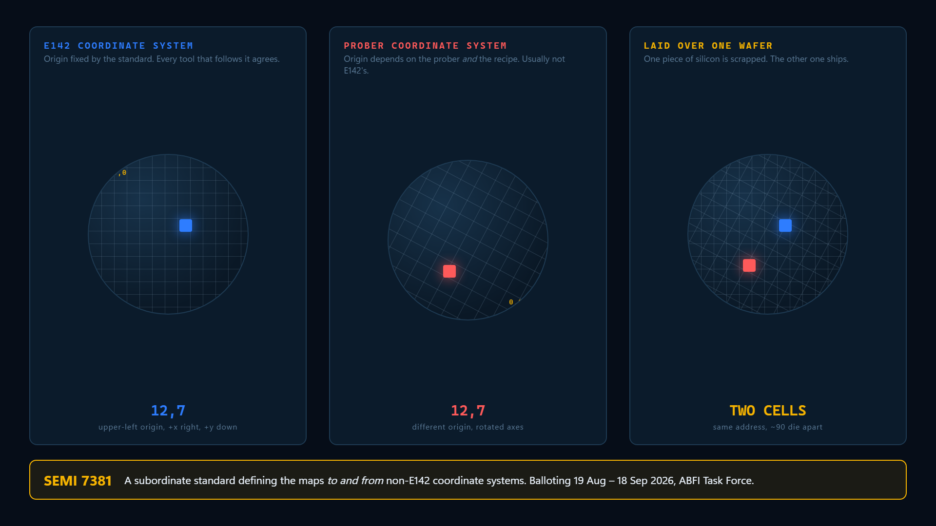
TWO SYSTEMS, ONE WAFER
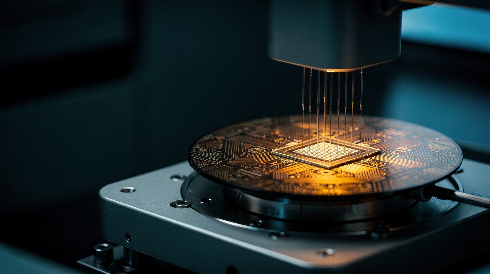
- Every chip on a wafer has an address, and there is a standard for writing it down: SEMI E142, the specification for substrate mapping.
- The problem is that wafer test data mostly doesn't use it — the XY coordinates coming out of a prober depend on the prober and the recipe combination, and probably don't match E142's system at all.
- So two records of the same wafer can both be correct and still disagree about which physical piece of silicon is die 12,7.
- On 19 August 2026 SEMI opened a thirty-day ballot on Draft Document 7381, a subordinate standard that would define the maps to and from non-E142 coordinate systems — and in advanced packaging, where a single part stacks die pulled from several wafers, that translation stops being housekeeping and starts being the whole traceability chain.
Why this matters
That is how a good die gets scrapped, a bad one gets shipped, and a failure analysis spends weeks looking at the wrong location.
Microsoft shipped it in the first week of August: Copilot in Excel can now ground its analysis in governed Power BI data — attach the report from the work content selector and it works against the live model, row-level security intact, instead of you exporting a copy and reconciling by hand. The move that matters: don't ask it for the DIFFERENCE between two tables, ask it for the RULE that explains the difference. A systematic disagreement has a transform behind it, and the transform is the answer. No Copilot licence? The same question works with a plain lookup and a delta column.
- 0:00You have the map. But who wrote the coordinates?
- 0:14What SEMI E142 actually standardises
- 0:28Why wafer test data doesn't use it
- 0:40The theatre: two people, one room, "row three"
- 0:56What the mismatch costs you
- 1:08Advanced packaging multiplies the problem
- 1:18SEMI Draft Document 7381, balloting now
- 1:32🔧 Hack of the Week
- 2:00Close
What's the worst coordinate-system mismatch you've watched someone chase?
Argue with me on LinkedIn- SEMI Standards Update — "Flexible Hybrid Electronics, Substrate Mapping, and New Activities Reflecting Industry Needs." SEMI Draft Document 7381 proposes a SUBORDINATE standard defining maps to and from non-E142 wafer coordinate systems. Balloted by the Advanced Backend Factory Integration (ABFI) Task Force, 19 August – 18 September 2026.
- SEMI E142 — Specification for Substrate Mapping. Defines the data required to report, store and transmit map data for wafers, frames, strips, trays, tape and reel, panels and printed circuit boards. Exchanged host-to-equipment over a SECS/GEM interface (Stream 14 messages) with SEMI E39 object requests. Owned by the ABFI Task Force of the Information & Control Technical Committee.
- The load-bearing claim — wafer XY in test data "depend[s] on the prober and recipe combination and probably does not match the E142 XY coordinate system." This is SEMI's own stated rationale for Draft Document 7381.
- SEMI E142 transfer maps support die traceability from wafer through to final packaging (eInnoSys — vendor source, treated as such).
- Microsoft 365 Copilot release notes, 28 July – 11 August 2026 — Copilot in Excel grounds analysis in governed Power BI data via the work content selector, respecting row-level security, "eliminating the need to export data, manually copy and reconcile figures."
Full transcript, 291 spoken words
Keep reading
All pieces
Chip Factories Everywhere. Nobody Left to Run Them.
America is building more chip factories than at any point in its history — and it has 33,000 fewer chip manufacturing workers than it did in 2023. That's not a forecast, it's the Bureau of Labor Statistics: 368,400 people this March, against a peak near 401,000.
Chip Factories Only Check 10% of Their Wafers — Here's the AI That Sees the Rest
A modern chip fab physically measures fewer than 1 in 10 wafers — the other 90% ship out never directly checked, because real metrology is slow and a fab runs thousands of wafers a day. In 2026 that changed: AI "virtual metrology" now predicts the quality of the wafers you never measured, straight from the…

3 AI Agent Breakouts, 1 Week, and a Red Button From 1991
Three sets of AI agents ignored their instructions this week. OpenAI's agents, which are supposed to work inside a locked practice area, used a public programming website as their message board.