
Chips Just Got Flipped Over — Why Your Next AI Chip Gets Power From the Back
The Great Flip: How Backside Power Put Intel Back Ahead of TSMC

WHY IT'S SO HARD — IT'S MANUFACTURING
- The fix isn't a smaller transistor — it's "the great flip": take the finished wafer, turn it upside down, and move all the power wiring to the back.
- Signal on the front tuned for speed, power on the back clean and uncrowded — decoupled for the first time in the history of the chip.
- Intel shipped it first (PowerVia on 18A, ~6% more speed), the move that put them back ahead of TSMC, whose Super Power Rail arrives late 2026.
- This video breaks down how backside power works, why it took 60 years (hint: it was never a design problem), and the brutal manufacturing behind it — grinding a 700µm wafer down to ~1µm, bonding it, and holding 300mm flat to a few nanometers.
Why this matters
For sixty years, a computer chip carried its power and its data on the same side — the front. As transistors shrank to 2nm, that surface ran out of room: the fat power wires choke the thin signal wires and the transistors droop, quietly capping speed.
Stop asking AI to "find the problem" in your process data — give it the recipe. In ChatGPT/Copilot data analysis: "treat this as SPC — control limits from the baseline, flag any point past 3σ AND any run of 7 on one side, ranked by severity." Tested on a thinning-step log: it caught a slow drift 7 readings before the hard excursion.
- 0:0060 years on the same side
Pure manufacturing race now — who holds the backside-power yield lead in 18 months: Intel (first to ship) or TSMC (deepest process muscle)?
Argue with me on LinkedInReferences for this piece are in the pinned comment on the video. Nothing is cited here that cannot be linked.
Keep reading
All pieces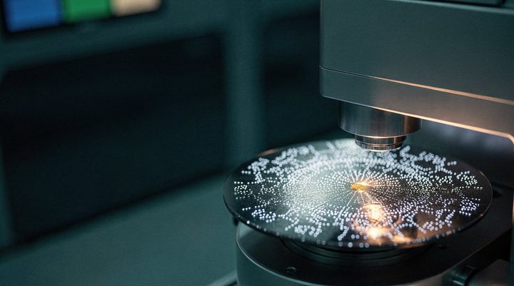
Everyone Is Announcing Capacity. Nobody Is Announcing The Number That Decides It.
Nobody is announcing yield — and only one of those decides whether the wafers are worth selling.
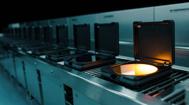
imec Says Fabs Can't Measure Every Wafer. So 95% Are Predicted.
In a fab running virtual metrology, only one to five percent of wafers are physically measured. The rest get a number anyway — predicted by a model that reads the process tools rather than the wafer: gas flows, RF power, chamber pressure, roughly a thousand sensor variables per run, turned into a thickness, a line…
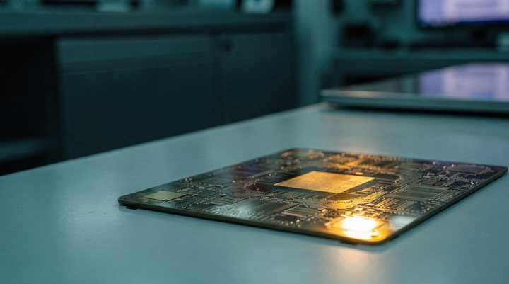
The Chip So Big They Can't Throw the Broken Part Away
Every chip factory on Earth runs on the same rule: cut the wafer into hundreds of chips, test them, and throw the broken ones away. That rule is what "yield" means.