
Chip Factories Only Check 10% of Their Wafers — Here's the AI That Sees the Rest
How Chipmakers Predict a Defect Before It Happens (Virtual Metrology, Explained)
This one has not been published to the channel yet. Subscribe on YouTube and it will turn up there.
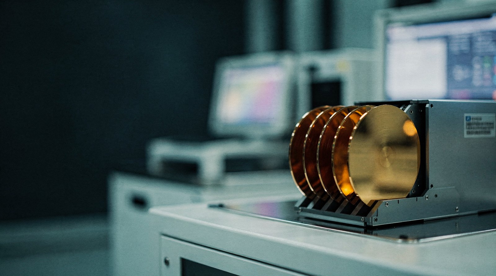
- A modern chip fab physically measures fewer than 1 in 10 wafers — the other 90% ship out never directly checked, because real metrology is slow and a fab runs thousands of wafers a day.
- In 2026 that changed: AI "virtual metrology" now predicts the quality of the wafers you never measured, straight from the sensor traces the tool already produces (pressure, temperature, RF power), lifting coverage from under 10% to full-wafer prediction and cutting root-cause from days to hours.
- The honest catch: a virtual model is only as good as the wafers you DID measure, so a chamber change can blind it until you re-reference — it augments physical metrology, it doesn't replace it.
- The non-obvious part for practitioners: virtual metrology isn't a new machine, it's a software layer riding your existing FDC data (no line change, no cloud, no MES rip-out) — the engineer who owns the data owns the model.
Why this matters
This year it moved onto the tool itself as edge AI — inference in milliseconds, on-premises, with nothing leaving the fab.
GPT-5.6 (launched Jul 8) leveled up data analysis. Drop a messy equipment log / shift CSV in and ask it to "find the drifting signals and rank my 3 worst chambers" — you get a ranked Pareto in ~30 seconds.
- 0:00Fabs only measure <10% of wafers
Virtual metrology on your line: would you let it auto-adjust the process, or only ever trust it as a second opinion?
Argue with me on LinkedInReferences for this piece are in the pinned comment on the video. Nothing is cited here that cannot be linked.
Full transcript, 218 spoken words
Keep reading
All pieces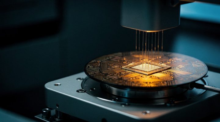
Your Chip Factory Can't Agree Which Die Failed
Every chip on a wafer has an address, and there is a standard for writing it down: SEMI E142, the specification for substrate mapping. The problem is that wafer test data mostly doesn't use it — the XY coordinates coming out of a prober depend on the prober and the recipe combination, and probably don't…
imec Says Fabs Can't Measure Every Wafer. So 95% Are Predicted.
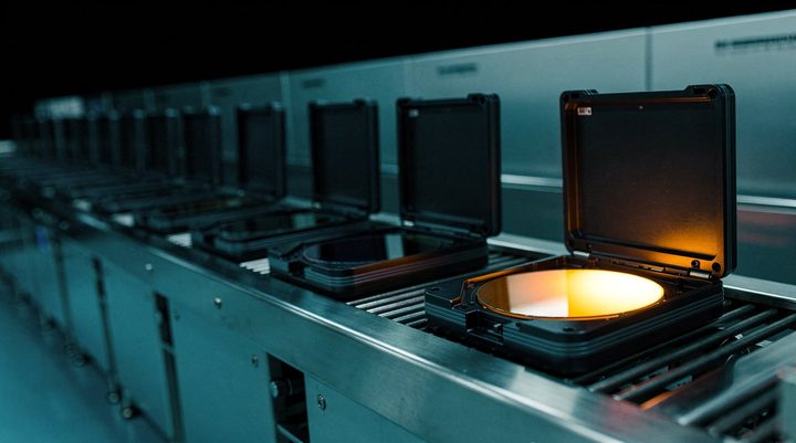
In a fab running virtual metrology, only one to five percent of wafers are physically measured. The rest get a number anyway — predicted by a model that reads the process tools rather than the wafer: gas flows, RF power, chamber pressure, roughly a thousand sensor variables per run, turned into a thickness, a line…
AI Now Lets Chip Fabs "Measure" Wafers They Never Touch (Virtual Metrology)
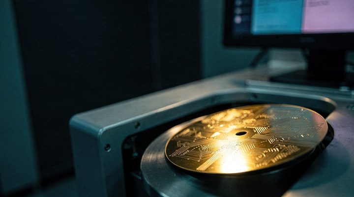
Chip factories physically measure only about 3 wafers in 100. For the other 97, an AI called virtual metrology predicts the exact dimension straight from the process tool's own sensor "fingerprint" — pressure, power, gas flow, hundreds of signals per wafer — in milliseconds, with no measurement step and no throughput hit.