
The 6-Inch Wafer That Every AI Data Center Depends On
NVIDIA Just Put $2B Into a Factory Running 1990s-Size Wafers — Here's Why
This one has not been published to the channel yet. Subscribe on YouTube and it will turn up there.
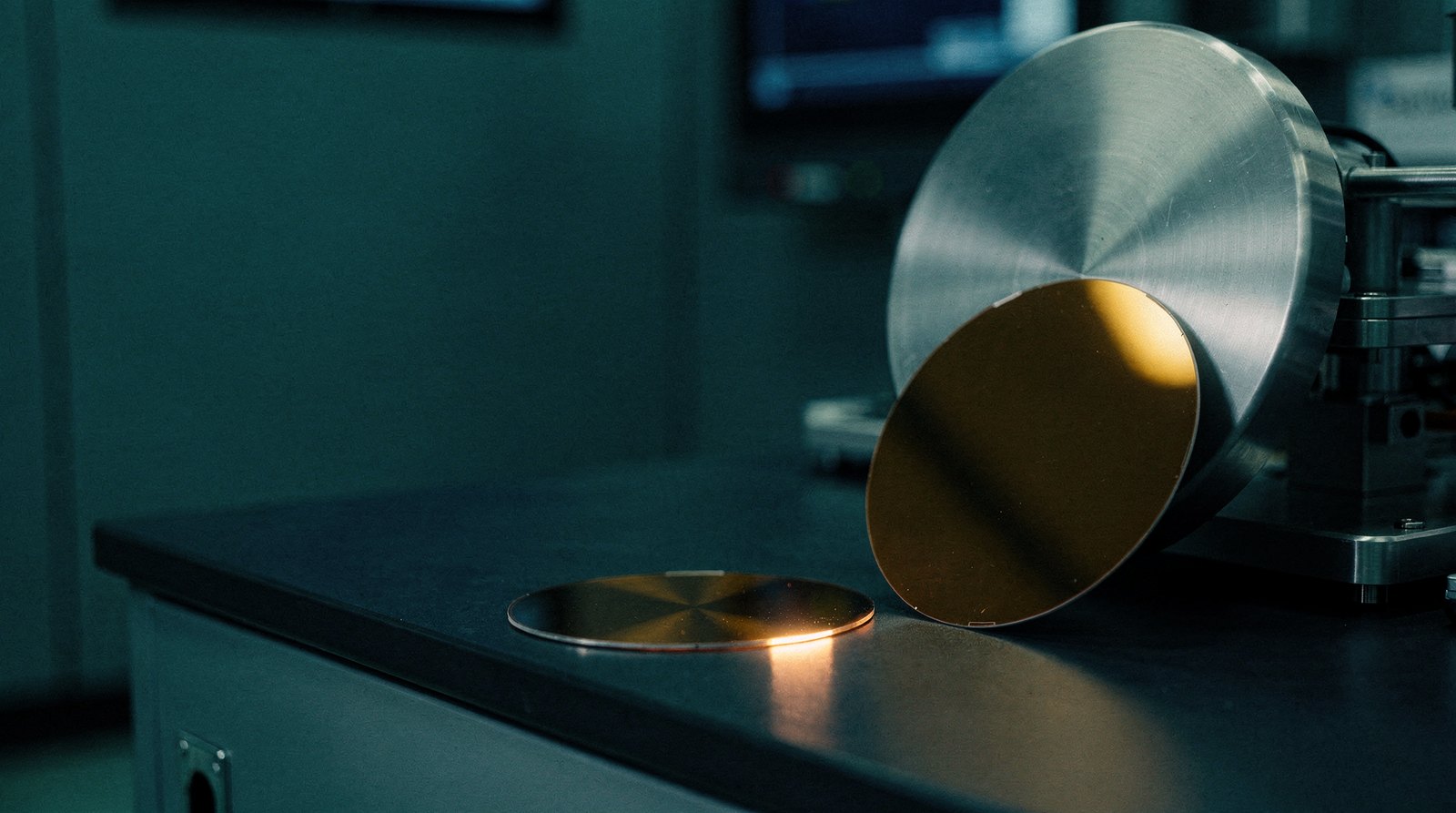
- NVIDIA just put $2 billion into a chip factory that runs six-inch wafers — not the twelve-inch wafers the rest of the industry moved to decades ago.
- The reason is that the chips moving data between processors inside an AI data center aren't silicon at all: they're indium phosphide, and the lasers built on it carry every high-speed optical link in the building.
- This video breaks down why the most strategically critical material in AI infrastructure is still made on 150mm wafers, what Coherent's $650M expansion in Sherman, Texas actually buys, and the part that matters most if you work in manufacturing — that compound semiconductors break the entire silicon yield playbook.
- In a silicon fab you lose yield across a thousand process steps and trace it backwards; in compound semiconductors the defects arrive in the crystal itself, which means the money is decided at crystal growth and epitaxy, before the fab really starts.
Microsoft has previewed run-only agent sharing in Copilot Studio (preview from August 2026, general availability January 2027). It lets you share an autonomous agent so colleagues can RUN it without being able to edit it, which keeps the people who build the automation separate from the people who benefit from it. If you work anywhere near a plant you have seen this pattern before, because it is recipe management: the process engineer owns the recipe, the operator runs it, and nobody rewrites it at three in the morning. So build the boring one first — the end-of-shift summary, the excursion write-up, the thing you retype every week — then share it run-only. Build it once and the whole team inherits your version, instead of eleven people quietly keeping eleven slightly different ones. If you are on the Microsoft 365 side rather than Copilot Studio, the same shape is available through Agent Builder: submit your agent to the Agent Store under "Built by your org", let an admin review and approve it, and it becomes discoverable across the organisation with governance attached.
- 0:00A $2B bet on six-inch wafers
- 0:16Why it isn't silicon
- 0:25What Coherent is building in Texas
- 0:41Where compound yield is really lost
- 0:53The flaw was already in the timber
- 1:17🔧 Hack of the Week: share it run-only (Copilot Studio)
Genuine question for the yield people — if the defect is already in the substrate, is downstream process control fighting a battle it can't win?
Argue with me on LinkedIn- NVIDIA — $2bn strategic investment in Coherent, March 2026, with a multiyear purchase commitment for laser and optical networking products.
- Coherent press release, 16 June 2026 — $650m project to quadruple indium phosphide wafer output on its 150mm line in Sherman, Texas; 1,000+ jobs.
- NIST / Commerce CHIPS Program Office, June 2026 — letter of intent, up to $50m to Coherent to expand that 150mm InP line.
- EDN and PDF Solutions, 2026 — compound-semiconductor yield: high defectivity originates in the raw substrate; SiC cost and yield concentrate at crystal growth and epitaxy; compound processes remain decades behind silicon CMOS in process maturity. (This last point is stated here rather than in the narration, where it was cut for length.)
- Microsoft Copilot Studio — run-only agent sharing ("Share Autonomous Agents to End Users"), preview from August 2026, general availability January 2027. Microsoft 365 Copilot — Agent Builder submissions to the Agent Store under "Built by your org" via admin review in the M365 Admin Center. No vendor endorsed. Coherent, NVIDIA and Microsoft are named because they are the actors in the story; nothing here characterises any of them negatively.
Full transcript, 285 spoken words
Keep reading
All pieces
imec Says Fabs Can't Measure Every Wafer. So 95% Are Predicted.
In a fab running virtual metrology, only one to five percent of wafers are physically measured. The rest get a number anyway — predicted by a model that reads the process tools rather than the wafer: gas flows, RF power, chamber pressure, roughly a thousand sensor variables per run, turned into a thickness, a line…

Your Fab's AI Goes Blind on the 2nm Node — Here's Why
Your fab's new AI spots defects better than any engineer — and on the brand-new node it goes almost blind. Not because the model is bad, but because every one of these systems learns from history: thousands of wafers, labelled defects, known-good outcomes.
NVIDIA Is Replacing the Wires Inside AI With Light — Here's the Real Catch
Inside a giant AI system, just moving the data between chips can burn more power than the computing itself — so NVIDIA is doing something wild: replacing the copper wires with light. In this video I break down co-packaged optics (the "light engine" built right into the chip package), why copper hit a hard power…